


Server-Online
137-1337-5955
13713375955
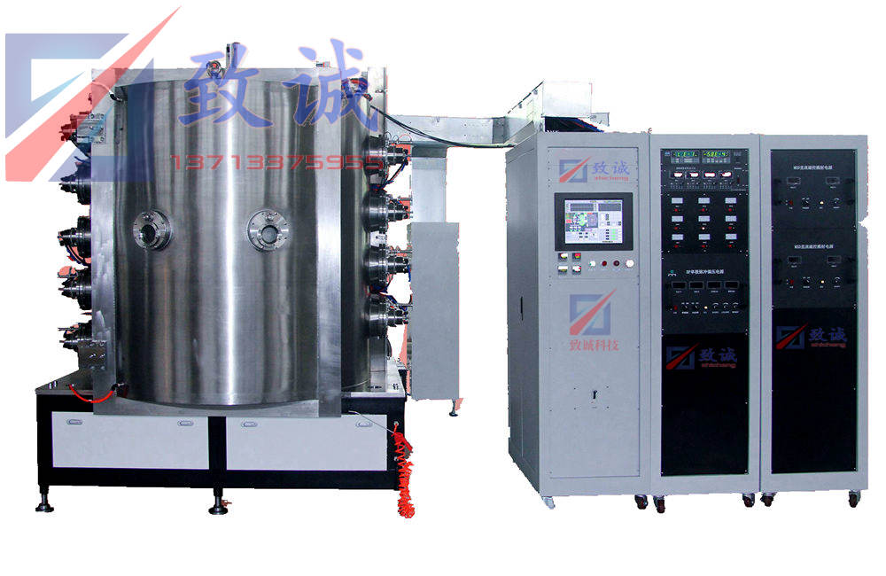
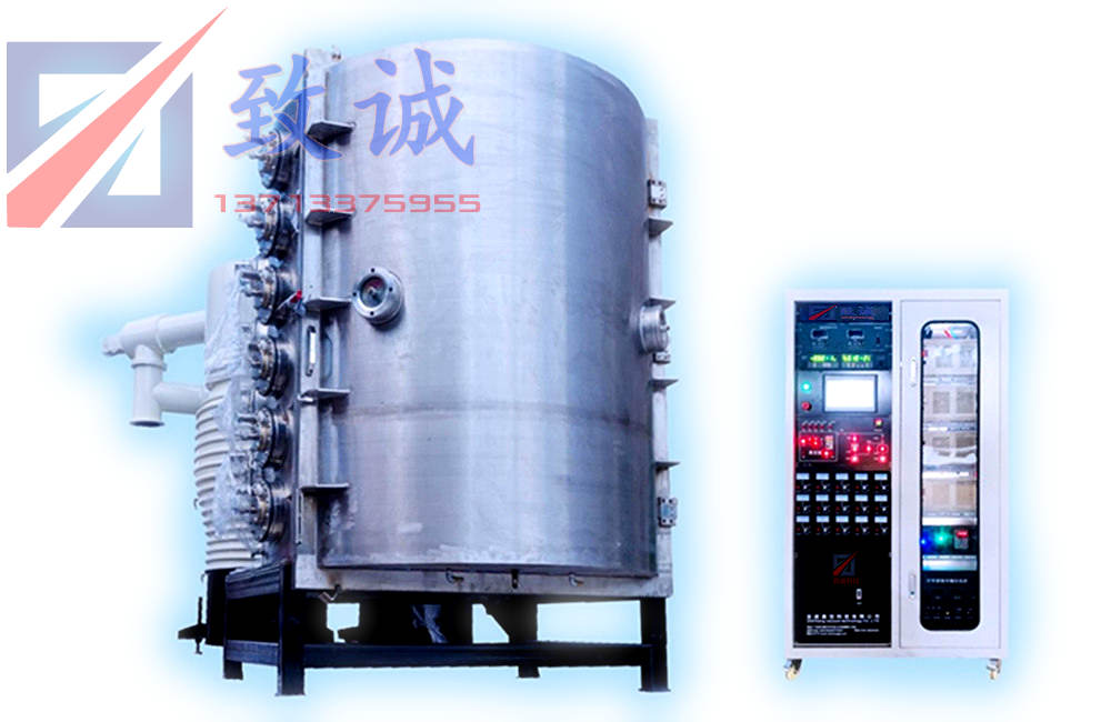
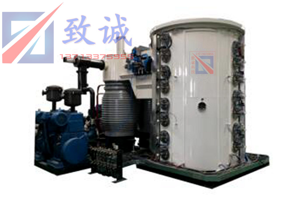
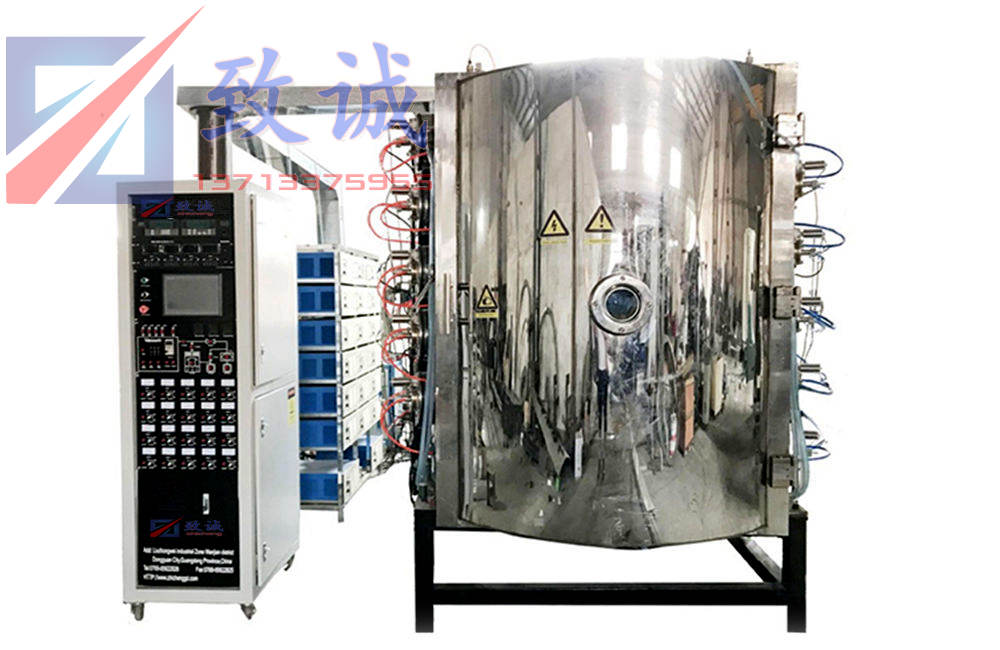
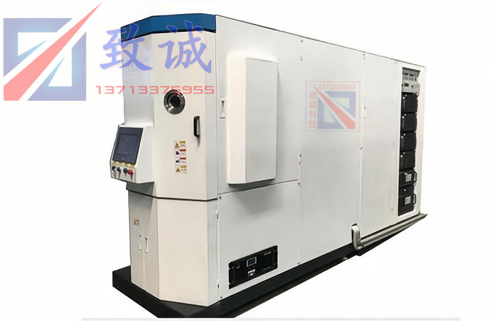
Electron beam evaporation
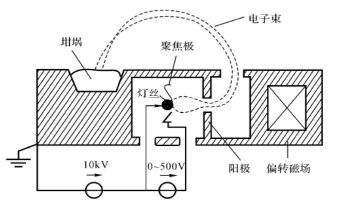
Electron beam evaporation is a method of vacuum evaporation coating, which is developed on the basis of tungsten wire evaporation. The method of directly heating the evaporating material under vacuum by using electron beam to vaporize the evaporating material and transport it to the substrate to form a film on the substrate. In the electron beam heating device, the heated material is placed in a water-cooled crucible, which can avoid the reaction between the evaporation material and the crucible wall affecting the quality of the film. Therefore, the electron beam evaporation deposition method can prepare high-purity films. At the same time, multiple crucibles can be placed in the same evaporation deposition device to achieve simultaneous or separate evaporation and deposition of a variety of different substances. Any material can be evaporated by electron beam evaporation. The electron beam is a high-speed electron flow. Electron beam evaporation is a mature and main coating method in the current vacuum coating technology, which solves the problem that the film material and the evaporation source material are easily mixed in direct contact in the resistance heating method.
Electron beam evaporation
Body with longitudinal beam scanning
The system with spray gun and full digital beam sweeper for single, multi pocket and large capacity crucible in thick layer.
Custom gun source with crucible turret system for special applications and extended product time between source maintenance.
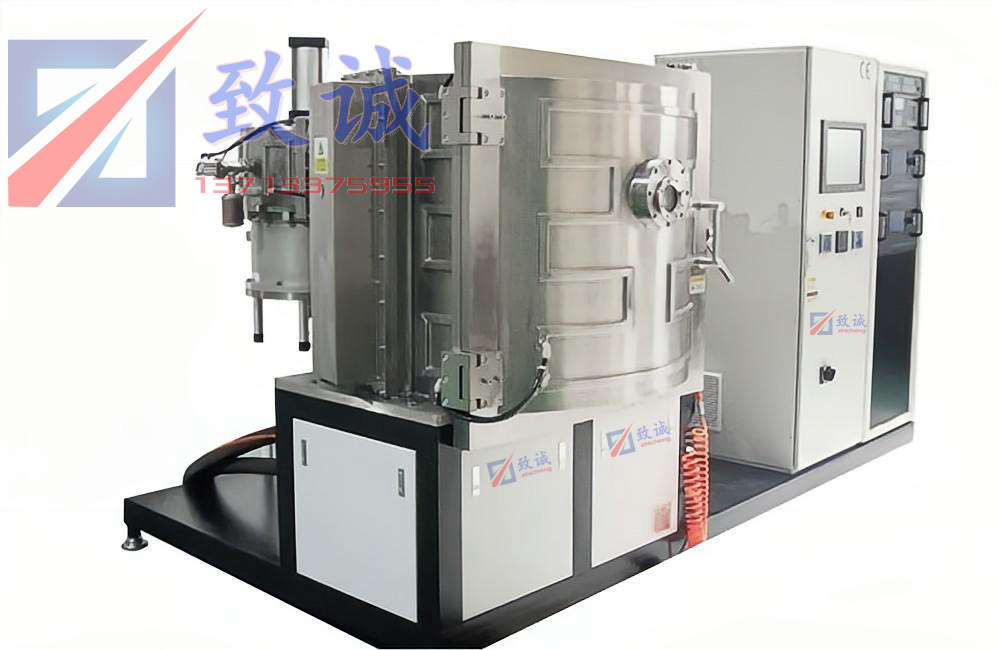
Ion assisted evaporation (IAD)
Ion source technology can provide lower process temperature, shorter process time and enhanced film performance for Photonics and optoelectronics applications.
advantage:
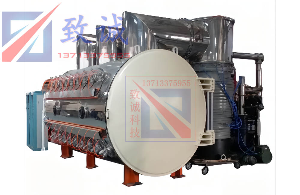
Electron beam evaporation can evaporate high melting point materials, which has higher thermal efficiency, higher beam density and faster evaporation speed than ordinary resistance heating evaporation. The prepared films have high purity, good quality, and can be controlled accurately. It can be widely used to prepare high-purity films, conductive glass and other optical materials.
The characteristic of electron beam evaporation is that it does not or rarely covers both sides of the target three-dimensional structure, and usually only deposits on the target surface. This is the difference between electron beam evaporation and sputtering.
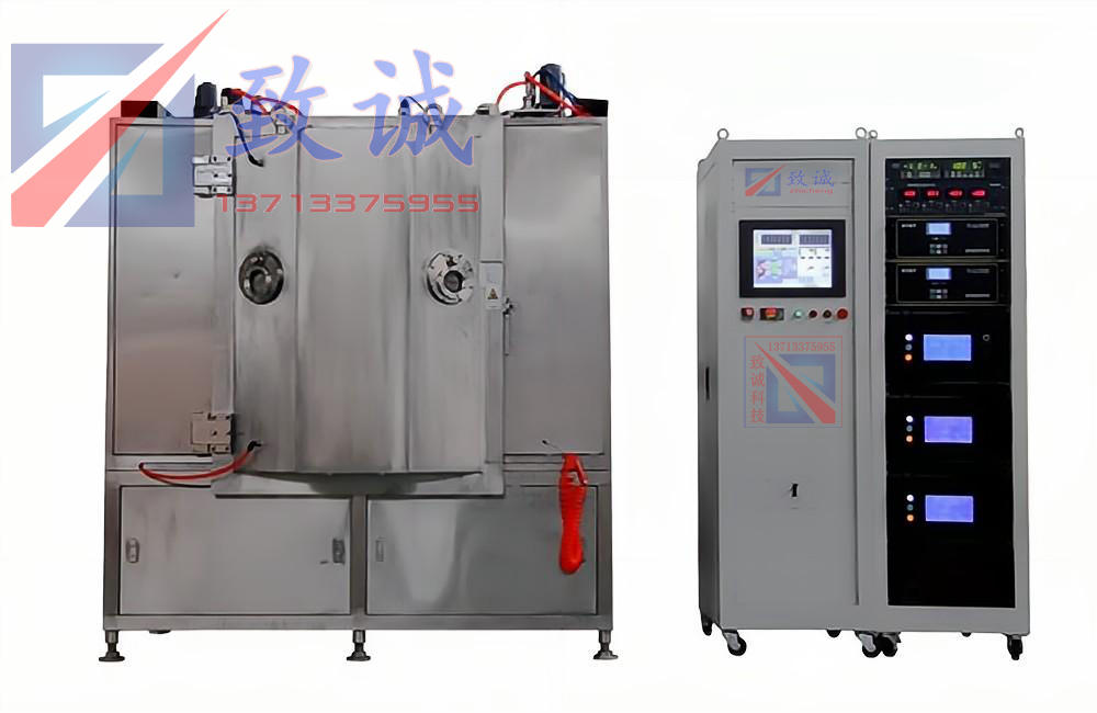
Application:
It is commonly used in semiconductor research and industry. The accelerated electron energy is used to strike the material target and make it evaporate. Finally, it's deposited on the target.
Dongguan City, Guangdong Province, China
+86 137-1337-5955
+86 13713375955 (Mr. Deng)
dgzhicheng@gmail.com
Copyright © 2022 Dongguan Zhicheng Technology Co., Ltd.